
← BFi53ER0 / BFi53ER0S EdgeRouter EdgeRouter · hardware

BFi53ER0 / BFi53ER0S hardware.

One design and one enclosure for both models, whichever solution it runs. The summary is below; the block diagram, the terminal-block pin definition and the full electrical and mechanical figures are in the hardware specification.
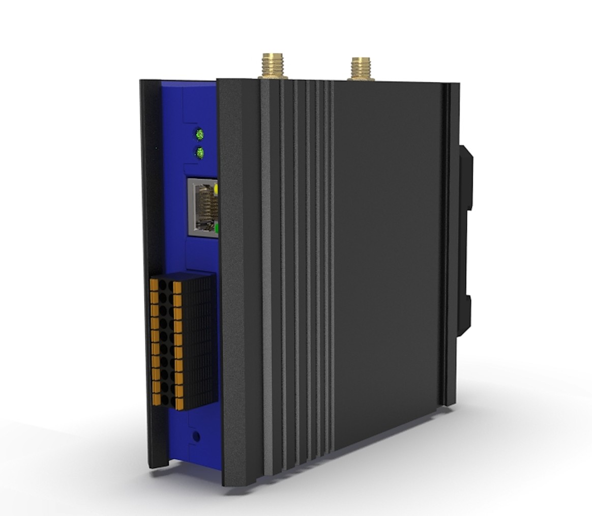
BFi53ER0 / BFi53ER0S EdgeRouter
Hardware summary

BFi53ER0 / BFi53ER0S

RadiosBluetooth 5.3 LE on both models · DECT NR+ on the BFi53ER0S
Field I/OBFi53ER0 terminal block (20-way, 2 × 10): RS-485 (Modbus RTU) · 2× 0–10 V in / out · 24 V digital I/O. BFi53ER0S: terminal assignment to be announced.
Network · power10/100 Ethernet · PoE+ or 14–32 V DC, from a Listed Class 2 supply or a Listed PoE switch or injector · 24 V field output, 0.65 A; the terminal block is Class 2 only, so mains loads are switched through relay contacts
Size · mounting119.6 × 110.0 × 37.4 mm, aluminium · DIN-rail or wall
DebugSWD header inside the enclosure · pinout in the hardware specification, section 3.3
TemperatureCore module BFi53MLG −40 ~ +105 °C
OriginMade in Taiwan by BANFi Semiconductor · patent applied for, patent pending
Download the hardware specification (PDF) ↓ Part numbers & order

FLS-HS-ER0 v3.2 · 11 pages · block diagram, pin definition, SWD debug header (section 3.3), electrical, mechanical, certification, ordering.

Documentation & downloads

Manuals and specifications.

The Quick Start, the User Manual, the hardware specification and the example code download directly; for the System Integration Guide, leave your company details in a short form. All FLSEMI documents →
Quick Start cover
Download · PDFQuick Start

What the gateway does, a first installation, the status light, the live view, and integration at a glance — ports and the Modbus register blocks in outline.

BFi53ER0-BF firmware 0.57.82 · v1.8 · 9 pages
Hardware specification cover
Download · PDFHardware specification

BFi53ER0 / BFi53ER0S: block diagram, terminal layout, SWD debug header, electrical, mechanical, certification and ordering.

FLS-HS-ER0 v3.2 · 11 pages
Python 3
Download · ZIPExample code

Receive every telegram over UDP, read the TCP feed with catch-up, and make a first Modbus TCP read — standard library only, free to use, copy and modify for BFi53ER0 integration.

3 programs + README · v1.1
Manuals
Download · short form
  • User ManualInstallation, every settings page, Modbus TCP, RS-485, the terminals, rules and alerts, time and history, backup, updates and troubleshooting — now a direct download. v3.6 · 58 pages.Download ↓
  • System Integration GuideJSON payload decoding, the complete Modbus register map and command reference. Leave your company details and we send it.Get the guide →

Firmware updates. Firmware images and their release notes are not published on this site. Write to hello@flsemi.us with the model, part number and firmware version on the System page, and we send what applies.
Core silicon

The chips at the heart of it.

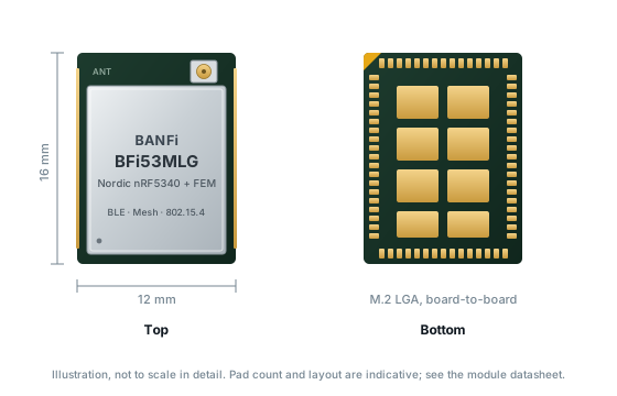
BFi53MLG module illustration, 12 by 16 mm M.2 LGA: top view with shield can and antenna connector, bottom view with LGA pads
Both models · core module

BANFi BFi53MLG — Nordic Semiconductor nRF5340 + FEM

−40 to +105 °Cindustrial temperature rating of the core module
ProcessorDual Arm Cortex-M33 — application core 128 MHz, network core 64 MHz
Memory1 MB flash, 512 KB RAM, 2 MB QSPI flash; network core 256 KB flash, 64 KB RAM
SecurityArm TrustZone, CryptoCell-312
Radio2.4 GHz Bluetooth LE (Mesh, Long Range) and IEEE 802.15.4, through the on-board front-end module
Package12 × 16 mm, M.2 LGA board-to-board
Module approvalsNCC · CE · FCC · IC · TELEC · NBTC · Bluetooth

The −40 to +105 °C figure is the core module’s own rating.
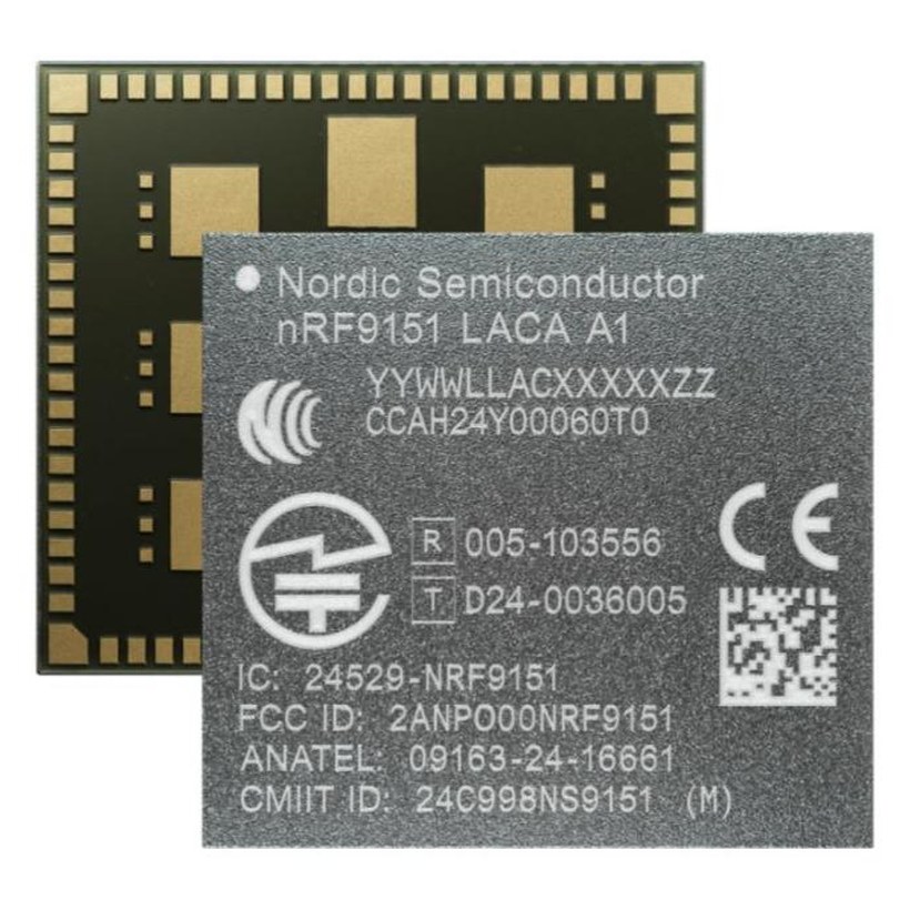
Nordic Semiconductor nRF9151 System-in-Package
BFi53ER0S · DECT NR+ radio

Nordic Semiconductor nRF9151

RoleDECT NR+ radio running our own BFi91NR7DLCVG stack (ETSI TS 103 636)
Bands1.9 GHz (band 1) and 915 MHz (band 4), chosen at start-up
Transmit power+21 dBm at 1.9 GHz, +19 dBm at 915 MHz
System block diagram

How the parts connect.

System block diagram: power (PoE+ or DC into an isolated flyback, 24 V field output, 3.3 V and 12 V rails), the BFi53MLG module with its 2.4 GHz front end and Ethernet controller, the nRF9151 DECT NR+ radio on the BFi53ER0S, and the field interfaces of the BFi53ER0: RS-485, analog in and out, digital in and out

The dashed block is fitted on the BFi53ER0S only; the field interfaces shown are those of the BFi53ER0. Pin definition, electrical and mechanical figures are in the hardware specification (PDF).

BFi53ER0 terminal block

BFi53ER0 terminal block (20-way, 2 × 10).

Front view with the Ethernet port below: odd terminals on the left with 01 at the top, even terminals on the right with 02 at the top. Terminal names match the case label. BFi53ER0S: terminal assignment to be announced.
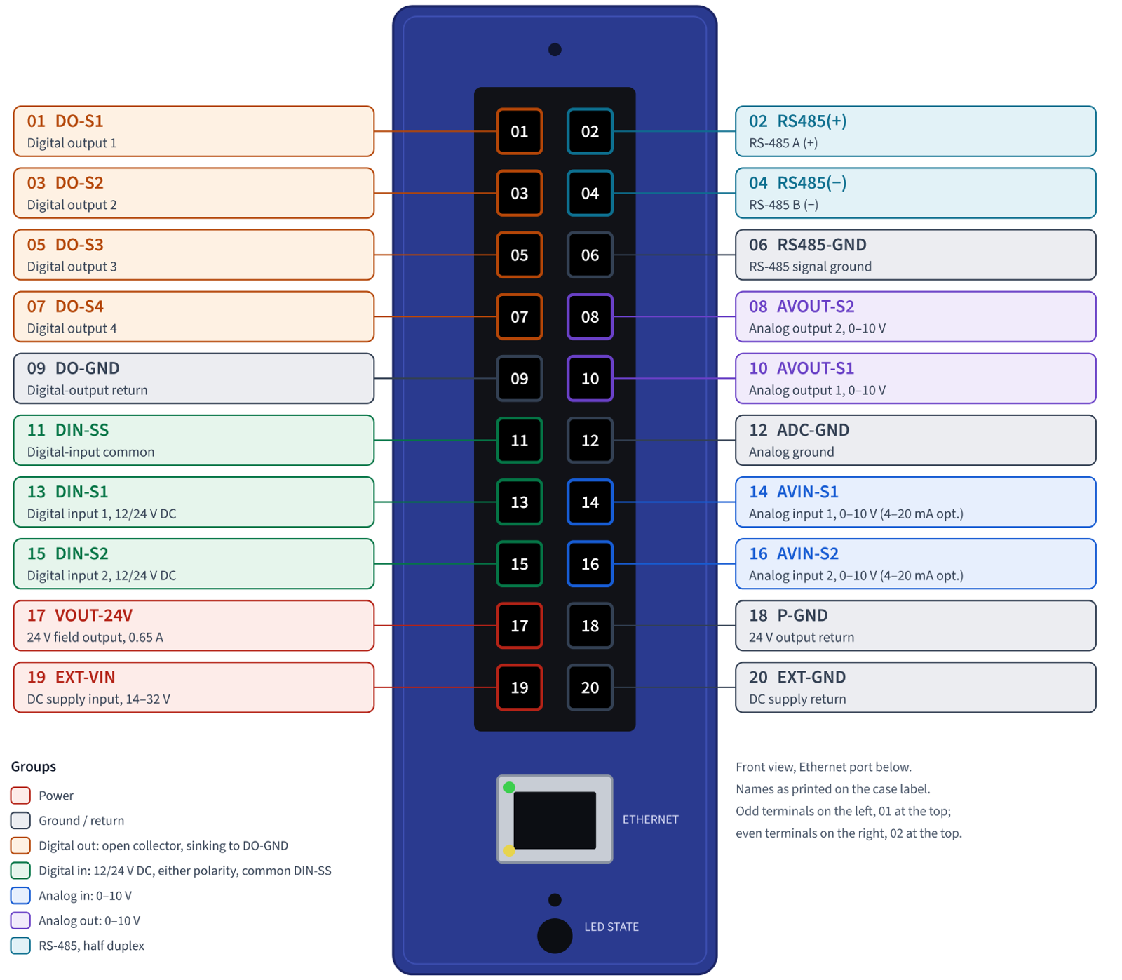
BFi53ER0 terminal block (20-way, 2 × 10), front view: 01 DO-S1, 03 DO-S2, 05 DO-S3, 07 DO-S4, 09 DO-GND, 11 DIN-SS, 13 DIN-S1, 15 DIN-S2, 17 VOUT-24V, 19 EXT-VIN on the left; 02 RS485(+), 04 RS485(−), 06 RS485-GND, 08 AVOUT-S2, 10 AVOUT-S1, 12 ADC-GND, 14 AVIN-S1, 16 AVIN-S2, 18 P-GND, 20 EXT-GND on the right